
Top articles
- Wear-Resistant Ceramic Tiles: Industrial Wear Protection Solution
- New Benchmark in Impact Resistance and Wear Protection:Three-in-One Ceramic Vulcanized Liners
- Wear-Resistant Ceramic Liners for Cyclone Separators
- What is a wear-resistant ceramic composite pipe?
- Performance Advantages and Application Fields of Alumina Ceramic Tubes
- Wear-Resistant Alumina Ceramic Liner Plate: Technical Specifications and Application Overview
- Wear-Resistant Alumina Hexagonal Ceramic Liner Tiles: A Reliable Choice for Industrial Wear Protection
- Wear-Resistant Alumina Ceramic Lining Bricks: A High-hardness, Long-Life Grinding Solution
- Alumina Ceramic Grinding Balls: High-Purity, Wear-Resistant Grinding Media
- Visit Us at UGOL ROSSII & MINING 2026 – Booth 1-D22
Latest articles
- Wear-Resistant Ceramic Tiles: Industrial Wear Protection Solution
- New Benchmark in Impact Resistance and Wear Protection:Three-in-One Ceramic Vulcanized Liners
- Wear-Resistant Ceramic Liners for Cyclone Separators
- What is a wear-resistant ceramic composite pipe?
- Performance Advantages and Application Fields of Alumina Ceramic Tubes
- Wear-Resistant Alumina Ceramic Liner Plate: Technical Specifications and Application Overview
- Wear-Resistant Alumina Hexagonal Ceramic Liner Tiles: A Reliable Choice for Industrial Wear Protection
- Wear-Resistant Alumina Ceramic Lining Bricks: A High-hardness, Long-Life Grinding Solution
- Alumina Ceramic Grinding Balls: High-Purity, Wear-Resistant Grinding Media
- Visit Us at UGOL ROSSII & MINING 2026 – Booth 1-D22
Your browsing history

Semiconductor-----Silicon Wafer Polishing
Semiconductor----Silicon Wafer Polishing
Briefly talk about the steps of silicon wafer polishing as below :
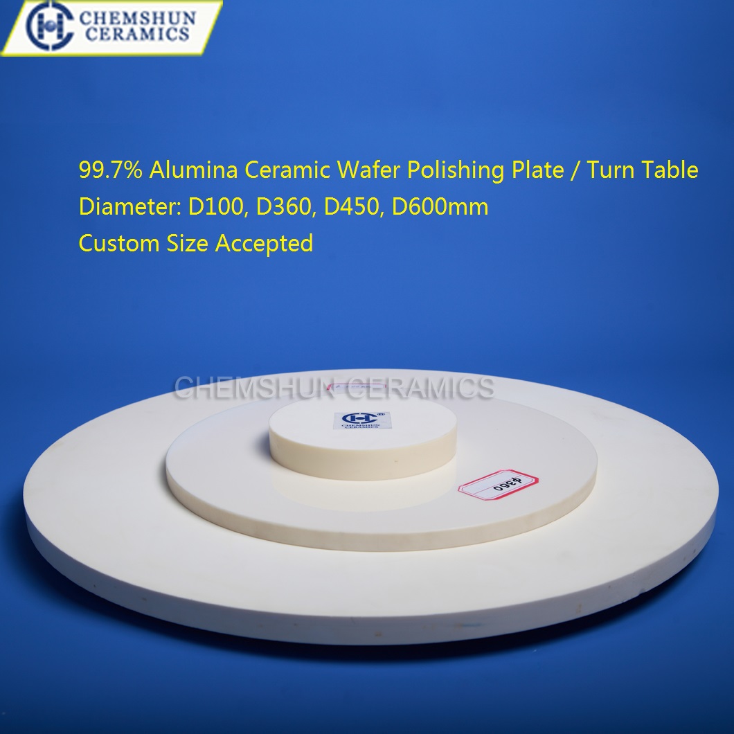
In the first step, the front side of the silicon wafer is treated, an adhesive is coated on the back of the silicon wafer, the silicon wafer is adhered to the ceramic board, the corrosion layer on the front surface of the silicon wafer is removed, and the silicon wafer is separated from the ceramic board by using a spatula, and cleaned and removed For the adhesive on the back of the silicon wafer, use a thickness measuring device to measure the thickness of the silicon wafer.
In the second step, the backside of the silicon wafer is treated, an adhesive is coated on the front of the silicon wafer, the silicon wafer is adhered to the ceramic board, the corrosion layer on the back of the silicon wafer is removed, and the silicon wafer is detached from the ceramic board with a spatula, and cleaned and removed Adhesive on the front of the silicon wafer to measure the flatness of the surface of the silicon wafer, and use a thickness measuring device to measure the thickness of the silicon wafer.
In the third step, the front surface of the silicon wafer is finally trimmed, an adhesive is coated on the back surface of the silicon wafer, the silicon wafer is adhered to the ceramic board, the corrosion layer on the front surface of the silicon wafer is removed, and the silicon wafer is detached from the ceramic board with a spatula and cleaned Remove the adhesive and particles from the back of the silicon wafer.